N channel jfet operation pdf Lynn Lake

InterFET Application Notes where (∆N)2 is the variance of the number of carriers N, and τ is the carrier lifetime. Above a certain frequency, the G-R noise power decreases as the square of frequency. When expressed as noise voltage, this means that it decreases at 6 dB/octave.
N-channel JFET Basics Learning about Electronics
MOSFET Construction and Operation. A p-channel JFET has a p-type semiconductor connecting the drain and source. If you apply a voltage to If you apply a voltage to the gate, no current flows gate …, JFET P-channel JFET Operation of JFET JFET terminals JFET drain curves JFET trans-conductance JFET biasing Ohmic region Active region MOSFET Depletion mode Enhancement mode Fig: J FET biase d fo r c o nduc tio n (c o mmo n so urc e co nfiguratio n) JFET operation Drain characteristic curves for JFET VGS controls ID EXAMPLE: For the JFET in the following figure, VGS(off)= 4v and ….
A p-channel JFET has a p-type semiconductor connecting the drain and source. If you apply a voltage to If you apply a voltage to the gate, no current flows gate … One type is n-channel and the other type is p-channel. Both types operate exactly the same way but the terminal voltages and currents are inverted. This discussion is for n-channel devices. JFET Basics 2 The main feature of JFETs is extremely high input resistance –usually at least several hundred megohms. This feature enables the power gain of a JFET amplifier to be huge. Development of
A p-channel JFET has a p-type semiconductor connecting the drain and source. If you apply a voltage to If you apply a voltage to the gate, no current flows gate … JFET Transistor N−Channel Features • These Devices are Pb−Free, Halogen Free/BFR Free and are RoHS Compliant MAXIMUM RATINGS Rating Symbol Value Unit Drain−Source Voltage VDS 25 Vdc Gate−Source Voltage VGS 25 Vdc Gate Current IG 10 mAdc Stresses exceeding those listed in the Maximum Ratings table may damage the device. If any of these limits are exceeded, device …
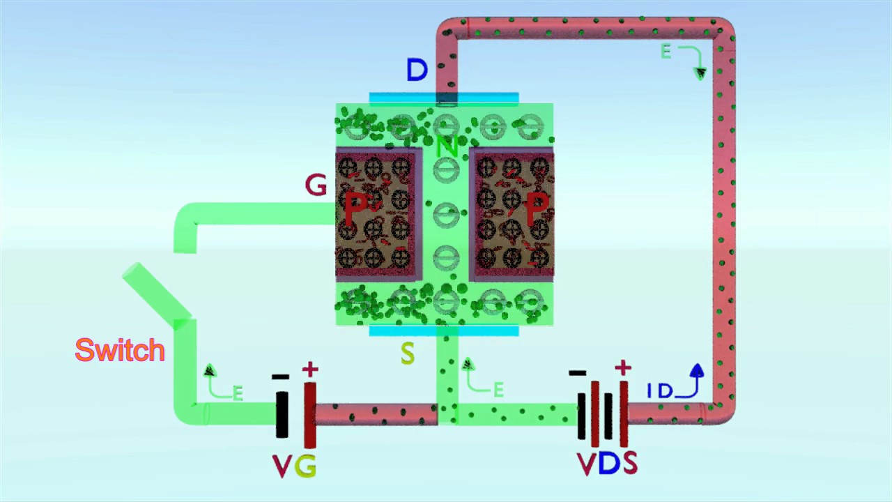
Working / Operation FET or JFET Gate are always in reverse biased, hence the gate current IG is practically zero. The source terminal is always connected to end of the drain supply, which provides the necessary carrier, in N- Channel JFET Source terminal is connected to … There are two basic configurations of junction field effect transistor, the N-channel JFET and the P-channel JFET. The N-channel JFET’s channel is doped with donor impurities meaning that the flow of current through the channel is negative (hence the term N-channel) in the form of electrons.
In a JFET, there is only one type of carrier,i.e. holes in p-type channel and electrons in n-type channel. For this reason it is also called unipolar transistor.However, in an ordinary BJT, both electrons and holes play role in conduction. Therefore, it is called as bipolar transistor. where (∆N)2 is the variance of the number of carriers N, and τ is the carrier lifetime. Above a certain frequency, the G-R noise power decreases as the square of frequency. When expressed as noise voltage, this means that it decreases at 6 dB/octave.
The LT®1057 is a matched JFET input dual op amp in the industry standard 8-pin configuration, featuring a combination of outstanding high speed and precision specifications. It replaces all the popular bipolar and JFET input dual op amps. In particular, the LT1057 upgrades the performance of systems using the LF412A and OP-215 JFET input duals. The LT1058 is the lowest offset quad JFET input The LT®1057 is a matched JFET input dual op amp in the industry standard 8-pin configuration, featuring a combination of outstanding high speed and precision specifications. It replaces all the popular bipolar and JFET input dual op amps. In particular, the LT1057 upgrades the performance of systems using the LF412A and OP-215 JFET input duals. The LT1058 is the lowest offset quad JFET input
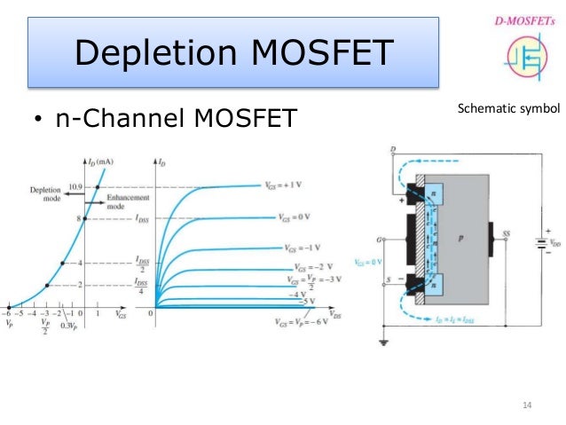
Working / Operation FET or JFET Gate are always in reverse biased, hence the gate current IG is practically zero. The source terminal is always connected to end of the drain supply, which provides the necessary carrier, in N- Channel JFET Source terminal is connected to … The n-channel depletion MOSFET (depletion NMOS) The depletion NMOS device is formed from a p-type substrate with physically implanted n-type source, drain and channel regions.
N-channel JFET Basics. A N-Channel JFET is a JFET whose channel is composed of primarily electrons as the charge carrier. This means that when the transistor is turned on, it is primarily the movement of electrons which constitutes the current flow. The n-channel depletion MOSFET (depletion NMOS) The depletion NMOS device is formed from a p-type substrate with physically implanted n-type source, drain and channel regions.
The LT®1057 is a matched JFET input dual op amp in the industry standard 8-pin configuration, featuring a combination of outstanding high speed and precision specifications. It replaces all the popular bipolar and JFET input dual op amps. In particular, the LT1057 upgrades the performance of systems using the LF412A and OP-215 JFET input duals. The LT1058 is the lowest offset quad JFET input N-channel JFET electron current flow from source to drain in (a) cross-section, (b) schematic symbol. Figure above shows a large electron current flow from (-) battery terminal, to FET source, out the drain, returning to the (+) battery terminal.
A p-channel JFET has a p-type semiconductor connecting the drain and source. If you apply a voltage to If you apply a voltage to the gate, no current flows gate … Basic operation of a JFET and n is the carrier concentration. For an n-channel JFET, I = N D eU D s where N D is the electron concentration ≈donor dopant concentration. • When approaching pinched-off, s becomes very small and U D has to become very large to maintain the current flow. The current density J = N D eU D becomes very high and under this condition the drift velocitybecomes
N-Channel JFET High Frequency Amplifier J308 – J310 / SST308 – SST310 FEATURES •Industry Standard Part in Low Cost Plastic Package •High Power Gain Working / Operation FET or JFET Gate are always in reverse biased, hence the gate current IG is practically zero. The source terminal is always connected to end of the drain supply, which provides the necessary carrier, in N- Channel JFET Source terminal is connected to …
N-Channel JFET Switch Datasheet catalog
JFET Basics. Working / Operation FET or JFET Gate are always in reverse biased, hence the gate current IG is practically zero. The source terminal is always connected to end of the drain supply, which provides the necessary carrier, in N- Channel JFET Source terminal is connected to …, Introduction to Junction Field-effect Transistors (JFET) Chapter 5 - Junction Field-effect Transistors A transistor is a linear semiconductor device that controls current with the application of a ….
JFET Construction and Operation
LSK489 Application Note CordellAudio.com. A JFET consists of a p-type or n-type silicon bar containing two pn junctions at the sides as shown in fig.1. The bar forms the conducting channel for the charge carriers. If the bar is of p-type, it is called p-channel JFET as shown in fig.1(i) and if the bar is of n-type, it is called n-channel JFET … The JFET Pierce crystal oscillator allows a wide frequency range of crystals to be used without circuit modification. Since the JFET gate does not load the crystal, good Q is.
A comparison between operation of an N-channel depletion-mode and enhancement-mode MOS devices is shown in Figure.3. Figure.3 The MOSFET is primarily a “transconductance” device where the input voltage and the output current are directly related, such that gate voltage (VG) is transferred to the source-drain current (IDS), and where Gm applies to its conductance. It is also a “unipolar Introduction to Junction Field-effect Transistors (JFET) Chapter 5 - Junction Field-effect Transistors A transistor is a linear semiconductor device that controls current with the application of a …
contrary, the p-channel JFET is formed by difussing one pair of n-type region into a slab of p-type material. In order to discuss the operation method of JFET, we hereby contrary, the p-channel JFET is formed by difussing one pair of n-type region into a slab of p-type material. In order to discuss the operation method of JFET, we hereby
N−Channel Junction Field Effect Transistors, depletion mode (Type A) designed for audio and switching applications. Features • N−Channel for Higher Gain • Drain and Source Interchangeable • High AC Input Impedance • High DC Input Resistance • Low Transfer and Input Capacitance • Low Cross−Modulation and Intermodulation Distortion • Plastic Encapsulated Package • Pb−Free EDC UNIT IV- Transistor and FET Characteristics Lesson-9: JFET and Construction of JFET. 2008 EDC Lesson 9- " , Raj Kamal, 2 1. Transistor. 2008 EDC Lesson 9- " , Raj Kamal, 3 Transistor Definition The transferred-resistance or transistor is a multi-junction device that is capable
TF2123 N-CHANNEL JFET Components datasheet pdf data sheet FREE from Datasheet4U.com Datasheet (data sheet) search for integrated circuits (ic), semiconductors and other electronic components such as resistors, capacitors, transistors and diodes. A JFET consists of a channel and a pn junction. The gate controls the depletion width of the pn The gate controls the depletion width of the pn junction and with that the conductance of the channel.
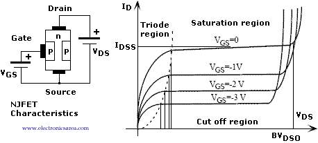
contrary, the p-channel JFET is formed by difussing one pair of n-type region into a slab of p-type material. In order to discuss the operation method of JFET, we hereby In the JFET the gate-channel contact is a reverse biased pn n-channel means The designation that the channel is . n. doped and the gate is . p. doped. The . p-channel is complement of . n-channel. Common Nomenc lature (n-channel FET example). Regions of JFET operation: Cut-off region: The transistor is off. There is no conduction between the drain and the source when the gate-source
U440/441 Vishay Siliconix www.vishay.com 8-2 Document Number: 70251 S-04031— Rev. D, 04-Jun-01 ˘ ˇ ˆ ˙ Limits U440 U441 Parameter Symbol Test Conditions Typ a Min Max Min Max Unit an n-channel power MOSFET. The parasitic JFET appearing between the two body implants restricts The parasitic JFET appearing between the two body implants restricts current flow when the depletion widths of the two adjacent body diodes extend into the drift region with
A p-channel JFET has a p-type semiconductor connecting the drain and source. If you apply a voltage to If you apply a voltage to the gate, no current flows gate … In the JFET the gate-channel contact is a reverse biased pn n-channel means The designation that the channel is . n. doped and the gate is . p. doped. The . p-channel is complement of . n-channel. Common Nomenc lature (n-channel FET example). Regions of JFET operation: Cut-off region: The transistor is off. There is no conduction between the drain and the source when the gate-source
The field-effect transistor (FET) is a transistor that uses an electric field to control the electrical behaviour of the device. FETs are also known as unipolar transistors since they involve single-carrier-type operation. In normal operating condition the drain terminal of n channel JFET is applied with positive potential and the drain terminal of a p channel JFET is applied with negative potential. The gate voltage is kept such in a JFET that the PN junction between the gate region and the channel is in reverse biased condition. The width of the depletion layer of this PN junction can be varied by varying gate
Basic operation of a JFET and n is the carrier concentration. For an n-channel JFET, I = N D eU D s where N D is the electron concentration ≈donor dopant concentration. • When approaching pinched-off, s becomes very small and U D has to become very large to maintain the current flow. The current density J = N D eU D becomes very high and under this condition the drift velocitybecomes the n-type substrate of Figure 1a leaving an n-type channel between the source and drain. (A complementary p-type device is made by reversing all of the material types.) These p-type regions will be used to control the current flow between the source and the drain and are thus called gate regions. As with any p-n junction, a depletion region surrounds the p-n junctions when the junctions are
This includes a basic description of the Junction FET (JFET) and the Metal Oxide FET (MOSFET), and also discusses N-Channel vs. P-Channel, as well as Depletion Mode and Enhancement Mode type devices. The function of the Gate, Source and Drain terminals are reviewed. The linear region and saturation region of operation of the devices is described and demonstrated. In a short video like … In Exercises 5.43 to 5.46, let the n-channel JFET have VP = –4 V and IDSS = 10 mA, and unless otherwise specified assume that in pinch-off (saturation) the output resistance is infinite. 5.43 For v GS =−2 V, find the minimum DS for the device to operate in pinch-off.
20/11/2016 · Analog Electronics: Working of JFET (Zero Voltage at the Gate) Topics Covered: 1. Working of junction field effect transistor. 2. Working of JFET when the voltage between gate and source is … The JFET is a long channel of semiconductor material, doped to contain an abundance of positive charge carriers or holes (p-type), or of negative carriers or electrons (n-type). Ohmic contacts at each end form the source (S) and the drain (D).
N-Channel JFET General Purpose Amplifier/Switch
N channel JFET junction field effect transistor YouTube. N-Channel JFET High Frequency Amplifier J308 – J310 / SST308 – SST310 FEATURES •Industry Standard Part in Low Cost Plastic Package •High Power Gain, Here an n channel JFET can be seen. This type is shown because it is more common than the alternative p channel JFET. However the same principles apply, the only changes that need to be made are that n-type material is replaced by p-type and so forth, and holes are used as the majority carriers instead of electrons..
Chapter 9 FET Amplifiers And Switching Circuits
Working of JFET (Zero Voltage at the Gate) YouTube. Working / Operation FET or JFET Gate are always in reverse biased, hence the gate current IG is practically zero. The source terminal is always connected to end of the drain supply, which provides the necessary carrier, in N- Channel JFET Source terminal is connected to …, Basic operation of a JFET and n is the carrier concentration. For an n-channel JFET, I = N D eU D s where N D is the electron concentration ≈donor dopant concentration. • When approaching pinched-off, s becomes very small and U D has to become very large to maintain the current flow. The current density J = N D eU D becomes very high and under this condition the drift velocitybecomes.
an n-channel power MOSFET. The parasitic JFET appearing between the two body implants restricts The parasitic JFET appearing between the two body implants restricts current flow when the depletion widths of the two adjacent body diodes extend into the drift region with Working of N - Channel Enhancement MOSFET is similar to that of P - Channel Enhancement MOSFET but only operationally and constructionally these two are different from each other. In N Channel Enhancement MOSFET a lightly doped p-type substrate forms the body of the device and source and drain regions are heavily doped with n-type impurities. Here also we connect the body …
2000 Jan 05 3 NXP Semiconductors Product specification N-channel junction FET BF862 LIMITING VALUES In accordance with the Absolute Maximum Rating System (IEC 134). The Symbol for N-channel and P-channel JFET’s are as follows n-channel FET p-channel FET The following are the important parameters of common
A comparison between operation of an N-channel depletion-mode and enhancement-mode MOS devices is shown in Figure.3. Figure.3 The MOSFET is primarily a “transconductance” device where the input voltage and the output current are directly related, such that gate voltage (VG) is transferred to the source-drain current (IDS), and where Gm applies to its conductance. It is also a “unipolar N-channel JFET electron current flow from source to drain in (a) cross-section, (b) schematic symbol. Figure above shows a large electron current flow from (-) battery terminal, to FET source, out the drain, returning to the (+) battery terminal.
A comparison between operation of an N-channel depletion-mode and enhancement-mode MOS devices is shown in Figure.3. Figure.3 The MOSFET is primarily a “transconductance” device where the input voltage and the output current are directly related, such that gate voltage (VG) is transferred to the source-drain current (IDS), and where Gm applies to its conductance. It is also a “unipolar 19.6 Difference Between JFET and Bipolar Transistor The JFET differs from an ordinary or bipolar transistor in the following ways : ( i ) In a JFET , there is only one type of carrier, holes in p -type channel and electrons in n -type
A p-channel JFET has a p-type semiconductor connecting the drain and source. If you apply a voltage to If you apply a voltage to the gate, no current flows gate … In normal operating condition the drain terminal of n channel JFET is applied with positive potential and the drain terminal of a p channel JFET is applied with negative potential. The gate voltage is kept such in a JFET that the PN junction between the gate region and the channel is in reverse biased condition. The width of the depletion layer of this PN junction can be varied by varying gate
the n-type substrate of Figure 1a leaving an n-type channel between the source and drain. (A complementary p-type device is made by reversing all of the material types.) These p-type regions will be used to control the current flow between the source and the drain and are thus called gate regions. As with any p-n junction, a depletion region surrounds the p-n junctions when the junctions are 2N5484 2N5485 2N5486 SILICON N-CHANNEL JFET The CENTRAL SEMICONDUCTOR 2N5484, 2N5485, and 2N5486 are silicon N-Channel JFETs designed for RF amplifier and mixer applications.
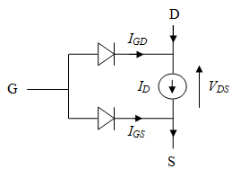
JFET Transistor N−Channel Features • These Devices are Pb−Free, Halogen Free/BFR Free and are RoHS Compliant MAXIMUM RATINGS Rating Symbol Value Unit Drain−Source Voltage VDS 25 Vdc Gate−Source Voltage VGS 25 Vdc Gate Current IG 10 mAdc Stresses exceeding those listed in the Maximum Ratings table may damage the device. If any of these limits are exceeded, device … The JFET must be biased with the gate-source junction reverse biased to prevent the flow of gate current, i.e. v GS <0 for the n-channel device and v GS >0 for the p-channel device. The gate current is then equal to the reverse saturation current of the junction.
N-Channel JFET High Frequency Amplifier J308 – J310 / SST308 – SST310 FEATURES •Industry Standard Part in Low Cost Plastic Package •High Power Gain 2N5484 2N5485 2N5486 SILICON N-CHANNEL JFET The CENTRAL SEMICONDUCTOR 2N5484, 2N5485, and 2N5486 are silicon N-Channel JFETs designed for RF amplifier and mixer applications.
A p-channel JFET has a p-type semiconductor connecting the drain and source. If you apply a voltage to If you apply a voltage to the gate, no current flows gate … MOSFET. In case of JFET, the gate must be reverse biased for proper operation of the device i.e. it can only have negative gate operation for n-channel and positive gate operation for p-channel.
EDC UNIT IV- Transistor and FET Characteristics Lesson-9: JFET and Construction of JFET. 2008 EDC Lesson 9- " , Raj Kamal, 2 1. Transistor. 2008 EDC Lesson 9- " , Raj Kamal, 3 Transistor Definition The transferred-resistance or transistor is a multi-junction device that is capable where (∆N)2 is the variance of the number of carriers N, and τ is the carrier lifetime. Above a certain frequency, the G-R noise power decreases as the square of frequency. When expressed as noise voltage, this means that it decreases at 6 dB/octave.
Working of JFET (Zero Voltage at the Gate) YouTube
N-Channel JFET General Purpose Amplifier/Switch. The JFET is a long channel of semiconductor material, doped to contain an abundance of positive charge carriers or holes (p-type), or of negative carriers or electrons (n-type). Ohmic contacts at each end form the source (S) and the drain (D)., 2N5484 2N5485 2N5486 SILICON N-CHANNEL JFET The CENTRAL SEMICONDUCTOR 2N5484, 2N5485, and 2N5486 are silicon N-Channel JFETs designed for RF amplifier and mixer applications..
N-channel JFET Basics Learning about Electronics
Buy JFETs Products Online Future Electronics. TF2123 N-CHANNEL JFET Components datasheet pdf data sheet FREE from Datasheet4U.com Datasheet (data sheet) search for integrated circuits (ic), semiconductors and other electronic components such as resistors, capacitors, transistors and diodes. MOSFET Construction and Operation MOSFET transistors have metal gates which are insulated from the semiconductor by a layer of SiO 2 or other dielectric. In enhancement type MOSFETs, the application of a gate voltage activates the channel (by inducing a layer of carriers between source and drain under the gate, Figure 121 )..
The Symbol for N-channel and P-channel JFET’s are as follows n-channel FET p-channel FET The following are the important parameters of common The JFET must be biased with the gate-source junction reverse biased to prevent the flow of gate current, i.e. v GS <0 for the n-channel device and v GS >0 for the p-channel device. The gate current is then equal to the reverse saturation current of the junction.
A JFET consists of a channel and a pn junction. The gate controls the depletion width of the pn The gate controls the depletion width of the pn junction and with that the conductance of the channel. The single channel junction field-effect transistor (JFET) is probably the simplest transistor available. As shown in the schematics below (Figure 6.13 in your text) for the n-channel JFET (left) and the p-channel JFET (right), these devices are simply an area of doped silicon with two diffusions of the opposite doping. Please be aware that the schematics presented are for illustrative
N-Channel MOSFET Basics A N-Channel MOSFET is a type of MOSFET in which the channel of the MOSFET is composed of a majority of electrons as current carriers. When the MOSFET is activated and is on, the majority of the current flowing are electrons moving through the channel. 2000 Jan 05 3 NXP Semiconductors Product specification N-channel junction FET BF862 LIMITING VALUES In accordance with the Absolute Maximum Rating System (IEC 134).
This includes a basic description of the Junction FET (JFET) and the Metal Oxide FET (MOSFET), and also discusses N-Channel vs. P-Channel, as well as Depletion Mode and Enhancement Mode type devices. The function of the Gate, Source and Drain terminals are reviewed. The linear region and saturation region of operation of the devices is described and demonstrated. In a short video like … stress ratings only and functional operation of the device at these or any other conditions above those indicated in the operational sections of the specifications is not implied.
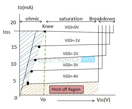
contrary, the p-channel JFET is formed by difussing one pair of n-type region into a slab of p-type material. In order to discuss the operation method of JFET, we hereby n-channel Jfet characteristics The junction gate field-effect transistor (JFET or JUGFET) is the simplest type of field. effect transistor. It can be used as an electronically-controlled switch or as a voltage-controlledresistance.
In the JFET the gate-channel contact is a reverse biased pn n-channel means The designation that the channel is . n. doped and the gate is . p. doped. The . p-channel is complement of . n-channel. Common Nomenc lature (n-channel FET example). Regions of JFET operation: Cut-off region: The transistor is off. There is no conduction between the drain and the source when the gate-source 2000 Jan 05 3 NXP Semiconductors Product specification N-channel junction FET BF862 LIMITING VALUES In accordance with the Absolute Maximum Rating System (IEC 134).
N-channel JFET electron current flow from source to drain in (a) cross-section, (b) schematic symbol. Figure above shows a large electron current flow from (-) battery terminal, to FET source, out the drain, returning to the (+) battery terminal. A JFET consists of a channel and a pn junction. The gate controls the depletion width of the pn The gate controls the depletion width of the pn junction and with that the conductance of the channel.
TF2123 N-CHANNEL JFET Components datasheet pdf data sheet FREE from Datasheet4U.com Datasheet (data sheet) search for integrated circuits (ic), semiconductors and other electronic components such as resistors, capacitors, transistors and diodes. 2000 Jan 05 3 NXP Semiconductors Product specification N-channel junction FET BF862 LIMITING VALUES In accordance with the Absolute Maximum Rating System (IEC 134).
The single channel junction field-effect transistor (JFET) is probably the simplest transistor available. As shown in the schematics below (Figure 6.13 in your text) for the n-channel JFET (left) and the p-channel JFET (right), these devices are simply an area of doped silicon with two diffusions of the opposite doping. Please be aware that the schematics presented are for illustrative In normal operating condition the drain terminal of n channel JFET is applied with positive potential and the drain terminal of a p channel JFET is applied with negative potential. The gate voltage is kept such in a JFET that the PN junction between the gate region and the channel is in reverse biased condition. The width of the depletion layer of this PN junction can be varied by varying gate
(b) Photograph of n-channel enhancement type MOSFET. From Fig 6.1 (a) it can be concluded that depletion type MOSFETs are normally ON type switches i.e, with the gate terminal open a nonzero drain current can flow in these devices. The field-effect transistor (FET) is a transistor that uses an electric field to control the electrical behaviour of the device. FETs are also known as unipolar transistors since they involve single-carrier-type operation.
Future Electronics is the leading distributor of Junction Field Effect Transistors (JFETs) from well-known manufacturers. Order now! stress ratings only and functional operation of the device at these or any other conditions above those indicated in the operational sections of the specifications is not implied.